Notes › EENG 3341: Microelectronics Lecture 6
Field Effect Transistors
714 words 5 min Modified
Table of Contents
Overview
- FETs are voltage-controlled semiconductor devices
- Terminals: Source (S), Gate (G), Drain (D), Body (B); in most circuits, the body is tied to the source
- The electric field from the gate voltage controls the current between drain and source
Types of FETs
- MOSFETs (Metal-Oxide Semiconductor FETs)
- Most widely used.
- PMOS: used in early designs.
- NMOS: higher performance due to electron mobility.
- CMOS: combines NMOS and PMOS for low power; dominant in digital circuits.
- JFETs (Junction FETs)
- Used in analog circuits, op-amps, and RF designs.
- Always depletion-mode.
MOSFETs
Characteristics
- Voltage-controlled, unipolar device.
- N-channel: electrons are carriers. P-channel: holes are carriers.
- Gate current ≈ 0 ($i_G = 0$).
- Body current ≈ 0 ($i_B = 0$).
Modes of Operation
-
Cutoff Region $v_{GS} \le V_{TN}$ ⇒ $i_D = 0$
-
Triode (Linear) Region $v_{GS} - V_{TN} > 0$ and $v_{GS} - V_{TN} > v_{DS}$ ⇒ $i_D = K_n[(v_{GS} - V_{TN})v_{DS} - \tfrac{v_{DS}^2}{2}]$
-
Saturation Region $v_{GS} - V_{TN} > 0$ and $v_{DS} > v_{GS} - V_{TN}$ ⇒ $i_D = \tfrac{K_n}{2}(v_{GS} - V_{TN})^2(1 + \lambda v_{DS})$
Where: $K_n = K_n' \tfrac{W}{L}$, $K_n' = \mu_n C_{ox}'$
Equivalent Circuit
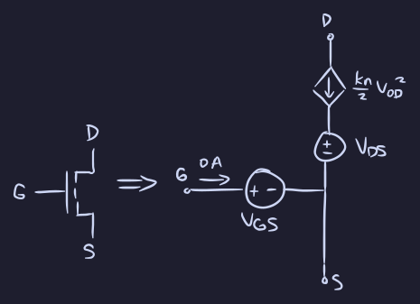
Channel-Length Modulation
- When $v_{DS} > v_{DSAT}$, channel shortens by $\Delta L$.
- Current slightly increases instead of saturating. $i_D = \tfrac{K_n'}{2}\tfrac{W}{L}(v_{GS} - V_{TN})^2(1 + \lambda v_{DS})$
- $\lambda$ (channel length modulation parameter): $0 \le \lambda \le 0.2 \text{ V}^{-1}$
- Usually $\lambda \approx 0$, so it is negligible
Transconductance ($g_m$)
- Defines how $i_D$ changes with $v_{GS}$:
- In triode region: $g_m = K_n v_{DS} = \frac{i_D}{v_{GS} - V_{TN} - \tfrac{v_{DS}}{2}}$
- In saturation region: $g_m = K_n (v_{GS} - V_{TN}) = \frac{2i_D}{v_{GS} - V_{TN}}$
- Larger $g_m$ → higher amplifier gain.
- $g_m$ is approximately twice as large in saturation as in triode.
Enhancement vs. Depletion MOSFETs
| Type | Channel Present at $v_{GS}=0$ | Turn-on Requirement | Common Use |
|---|---|---|---|
| Enhancement | No | $v_{GS} > V_T$ | Digital, CMOS |
| Depletion | Yes | $v_{GS} < 0$ (for n-channel) | Analog, older designs |
PMOS Transistors
- Built in n-type substrate with p-type source and drain.
- Requires $v_{GS} < V_{TP}$ (where $V_{TP} < 0$) for conduction.
- Follows similar I–V relationships as NMOS but with reversed polarities.
MOSFET as a Switch
- Off-state: $v_{GS} = 0$ → open circuit (cutoff region).
- On-state: $v_{GS} > V_{TN}$ → low $R_{DS}$ (triode region).
- Used in digital logic gates, such as CMOS inverters.
Biasing MOSFETs
Purpose
- To set a stable Q-point $(I_D, V_{DS}, V_{GS})$ for desired operation region.
- Bias defines the DC condition; signal varies around it. $v_{GS} = V_{GS} + v_{gs}$, $i_D = I_D + i_d$
Common Biasing Methods
| Bias Type | Description | Notes |
|---|---|---|
| Fixed $V_{GS}$ Bias | Uses constant gate-source voltage. | Simple but sensitive to $V_T$ and $K_n$ variations. |
| Load-Line Bias | Graphical method showing $I_D$–$V_{DS}$ relationship. | Helps visualize operation point. |
| Four-Resistor (Voltage Divider) | Uses feedback and voltage division for stability. | Common in analog design. |
| Drain (Two-Resistor) Feedback | Gate voltage from drain through resistor. | Improves Q-point stability. |
Bias Equation: $V_{DD} = I_D R_D + V_{DS}$
Example: Q-point Verification
-
Assume saturation: check if $V_{DS} > V_{GS} - V_{TN}$. If true, assumption correct.
-
For channel-length modulation: $i_D = \tfrac{K_n}{2}(V_{GS} - V_{TN})^2(1 + \lambda V_{DS})$
Biasing Summary
| Bias Type | Advantage | Limitation | Application |
|---|---|---|---|
| Constant $V_{GS}$ | Simple | High sensitivity | Switching |
| Four-Resistor | High stability | More components | Amplifiers |
| Drain Feedback | Moderate stability | Lower gain | Digital switching |
JFETs
Structure and Operation
- Depletion-mode device only.
- Current controlled by gate–source voltage ($v_{GS}$) through the channel.
- Terminals: Gate (G), Source (S), Drain (D).
- High input impedance, low noise.
I–V Relationships
For n-channel JFET:
-
Cutoff: $v_{GS} \le V_P$ ⇒ $i_D = 0$
-
Triode region: $i_D = \tfrac{2I_{DSS}}{V_P^2}\left[(v_{GS} - V_P)v_{DS} - \tfrac{v_{DS}^2}{2}\right]$
-
Saturation region (Pinch-off): $i_D = I_{DSS}\left(1 - \tfrac{v_{GS}}{V_P}\right)^2(1 + \lambda v_{DS})$
where
- $V_P$: pinch-off voltage
- $I_{DSS}$: drain current at $v_{GS} = 0$
Equivalent Circuit
- Same as MOSFET, but the dependent current source value is $i_{DSS} \left(\frac{V_{OD}}{V_{p}}\right)$ in pinch-off, where $V_{OD} \equiv V_{GS} - V_{p}$
Comparison: MOSFET vs. JFET
| Property | MOSFET | JFET |
|---|---|---|
| Gate control | Insulated gate (oxide) | PN junction gate |
| Modes | Enhancement and depletion | Depletion only |
| Input impedance | Very high | High |
| Fabrication | Easier, cheaper | Complex, costly |
| Common use | Digital & power circuits | Analog, low-noise amplifiers |
Key Equations Summary
-
Triode Region: $i_D = K_n[(v_{GS} - V_{TN})v_{DS} - \tfrac{v_{DS}^2}{2}]$
-
Saturation Region: $i_D = \tfrac{K_n}{2}(v_{GS} - V_{TN})^2(1 + \lambda v_{DS})$
-
Transconductance: $g_m = \tfrac{2i_D}{v_{GS} - V_{TN}}$
-
Bias Line: $V_{DD} = I_D R_D + V_{DS}$
References
- Course slides, chapter 4: Field-Effect Transistors
- Course slides, chapter 5: Bipolar Junction Transistors
Sources
- Course slides, chapter 4: Field-Effect Transistors
- Course slides, chapter 5: Bipolar Junction Transistors