Notes › EENG 3341: Microelectronics Lecture 9
Single-Transistor Amplifiers
923 words 5 min Modified
Table of Contents
Signal Injection and Extraction
BJT
- The forward-active region is characterized by $i_{C} = I_{S} \exp \left( \frac{V_{BE}}{V_{T}} \right)$
- This implies that $V_{BE}$ must be altered to induce a substantial change in the collector and emitter currents
- Since $V_{BE} = V_{B} - V_{E}$, the base and emitter terminals may be used to inject signal for amplification
- The output signal would be directly proportional to signal injected into the base port and inversely proportional to signal injected into the emitter port $(V_{BE} \propto V_{B}; V_{BE} \propto \frac{1}{V_{E}})$
- The collector voltage has negligible effect on the terminal currents, so we never use the collector terminal as an input
- This implies that $V_{BE}$ must be altered to induce a substantial change in the collector and emitter currents
- The induced collector/emitter currents go through a resistor, which changes the voltage across that resistor; this voltage may then be read as an output signal from the transistor
- Since there is usually no resistive load for which $i_{B}$ passes through to produce a voltage, we never use the base terminal as an output
MOSFET/JFET
- The pinch-off region for a MOSFET is characterized by $i_{S} = i_{D} =\frac{K_{n}}{2}V_{OD}^2$
- This implies that $V_{GS}$ must be altered to induce a substantial change in the drain/source current
- Since $V_{GS} = V_{G} - V_{S}$, the gate and source terminals are used to inject signal for amplification
- The response would be directly proportional to signal in the gate terminal and inversely proportional to signal in the source terminal
- The drain voltage has a negligible effect on the terminal currents, so we never use the drain as an input
- Can hook up a resistive load at the drain or source terminals and measure the potential difference for an output
- However, since $i_G$ is always zero, we never use the gate terminal for output
- This implies that $V_{GS}$ must be altered to induce a substantial change in the drain/source current
- For a JFET, the behavior is the exact same as a MOSFET; however, it has some slightly different parameters due to being a completely different device (such as $V_{p}$ and $i_{DD}$, which causes the pinch-off region to be characterized with a slightly different equation
- We don’t really care about this, since JFET is not going to be included in our study, but you can look at the characterization of JFET operation in the active mode Field Effect Transistors for more information
“Common” Notation
- When we say that a port is “common,” that just means that it’s not being fed any input or output
- Typically, the port that is common is grounded (either directly or indirectly via a voltage source or bypass resistor in AC analysis)
- Practically speaking, however, when it comes to single-transistor amps, we usually incorporate a feedback resistance of some kind between the common port and ground
- This allows for better moderation of the voltage/current gain, input/output resistances, and input signal range (such that linear amplification would still hold)
- We probably won’t be tested on this edge case, but nonetheless, it is always good practice to write the equivalent AC circuit when conducting the small signal analysis of these amp circuits
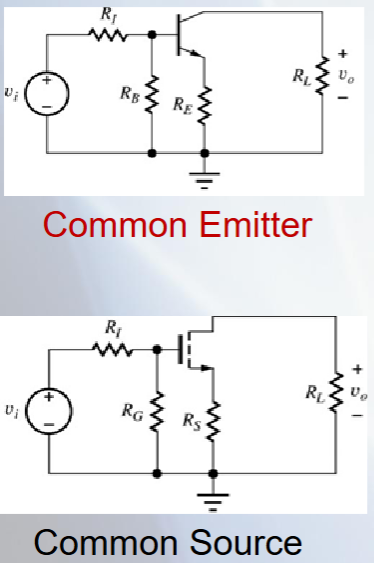
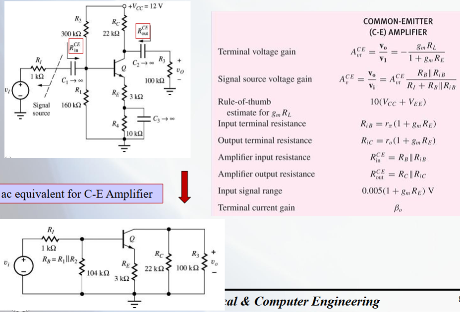
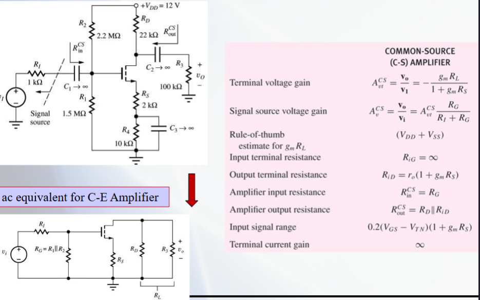
Inverting Amplifier
- Provides a high voltage gain with $180^{\circ}$ phase shift
- LHS input; RHS output; bottom common
- BJT: base input; collector output; common emitter
- MOSFET: gate input; drain output; common source
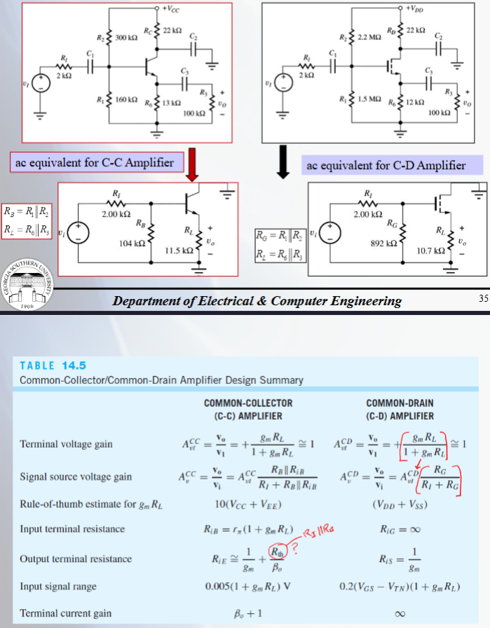
Follower Amplifier
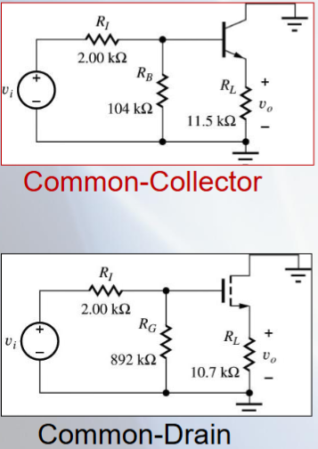
- Provides a voltage gain of unity
- LHS input; bottom output; RHS common
- BJT: base input; emitter output; common collector
- MOSFET: gate input; source output; common drain
- Has a high input resistance $(\rightarrow \infty)$ and low output resistance $(\rightarrow 0)$
- This allows for an input signal that is quite large without exceeding linearity constraints
- FETs have a higher input and output resistance than a BJT
- This means FETs have higher transconductances than BJTs
- Which implies that the voltage gain of a C-C BJT is closer to unity than a C-D FET, since $A_{vt} \approx \frac{g_{m}R_{L}}{1 + g_{m}R_{L}}$
- Tradeoff:
- If you want as close of a gain to unity as possible, use a BJT; however, you will lose some of the signal range due to the lower input resistance
- If you want to minimize distortion for higher signal ranges, and you are okay with losing some gain in the process, use a FET
- FETs are also more temperature-stable than BJTs and less-costly to manufacture
- Since FETs have theoretically infinite input resistance and current gain, they are also useful for input isolation
- This basically means you can electrically insulating the input and output voltages from one another, which prevents excessive current/power draw (safety hazard)
Non-inverting Amplifier
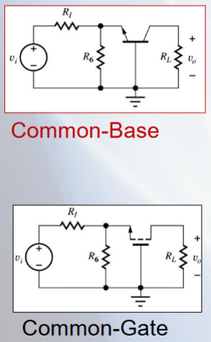
- Provides a voltage gain with no phase shift
- Much lower input resistance than inverting amp
- The configuration topology is a bit weird, since they usually reorient the circuit such that the transistor is facing up instead of to the right
- If that ever happens, you can basically assume it’s a non-inverting amp
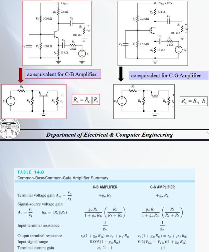
- BJT: emitter input; collector output; common base
- MOSFET: source input; drain output; common gate
- BJT and FET implementations have very similar gains in noninverting configuration
- BJT has higher output resistance and lower input resistance in general due to higher transconductance
- FET has higher range because $V_{OD}$ is much larger than $V_{T} = 0.7$
Multi-stage Amplifier Circuits
- Coupling capacitors are connected to the output terminal to chain multiple amplifiers together
- Steps for analysis
- Calculate small-signal parameters for each transistor
- You would have to be given the parameters and Q-Points for each transistor in order to do this step with ease
- If not, then you better perform DC analysis for each transistor! Pray your professor gives you the information for all transistors in each multi-stage amp circuit on the test
- Find the AC equivalent circuit
- Find the small-signal equivalent circuit
- ???
- Profit
- Calculate small-signal parameters for each transistor
- Lmao im so cooked
References
- Course slides, chapter 14: Single-Transistor Amplifiers
Sources
- Course slides, chapter 14: Single-Transistor Amplifiers